Diodes
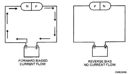
A diode (fig. 1-8) is a device that will allow current to pass through itself in only one direction. A diode can be thought of as an electrical check valve. Diodes are constructed by joining N-type material and P-type material together. The negative electrical terminal is located on the N-type material and the positive terminal is located on the P-type material.
When a diode is placed in a circuit, the N-material is connected to the negative side of the circuit and the positive side of the circuit is connected to the P-material. In this configuration, which is known as forward bias, the diode is a good conductor. This is because the positively charged holes in the P-type material move toward the junction and fill these holes using them to move across the P-material. If the connections to the diodes are reversed, current flow will be blocked. This design is known as reverse bias. When the diode is connected backwards, the positively charged holes are attracted away from the junction to the negative terminal and the free electrons in the N-material are attracted away from the junction to the positive terminal. Without the presence of holes at the junction, the electrons are not able to cross it.
Zener Diodes
A zener diode (fig. 1-9) is a special type of diode that conducts current in the reverse direction as long as the voltage is above a predetermined value that is built into the device during manufacturing. For instance, a certain zener diode may not conduct current if the reverse bias voltage is below 6 volts. As the voltage

Figure 1-8. - Diode operation.
increases to 6 volts or more, the diode suddenly will begin to conduct reverse bias current. This device is used in control circuits, such as voltage regulators.
Transistors
A transistor (fig. 1-10) is an electrical device that is used in circuits to control the flow of current. It operates by either allowing current to flow or not allowing it to flow. Transistors operate electronically and have no moving parts to perform their function. This design allows for a longer operating life of the component. The major automotive applications of transistors are for electronic ignition systems and voltage regulators.
The PNP transistor (fig. 1-11) is the most common design in automotive applications. It is manufactured by sandwiching an N-type semiconductor element between two P-type semiconductor elements. A positive charge is applied to one of the P-type elements. This element is called the emitter. The other P-type element connects to the electrical component. This element is called the collector. The third element, which is in the middle, is made of N-type material and is called the base. The application of low current negative charge to the base will allow a heavy current to flow between the emitter and the collector. Whenever the current to the base is switched off, the current flow from the emitter to the collector is interrupted also.
The NPN transistor (fig. 1-11) is similar to the PNP transistor. The difference is that it is used in the negative side of the circuit. As the term NPN implies,
Continue Reading