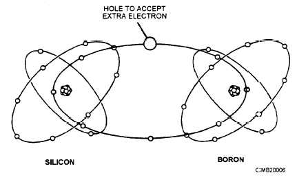
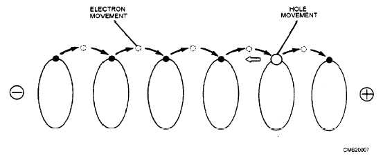
covalent bonding yields seven electrons in the outer shell. This leaves an opening for another electron and is shown in figure 1-6. This space is called a hole and can be considered a positive charge, just as the extra electrons that exist in N-type semiconductor material are considered a negative charge. Materials that have holes in their outermost electron shells are called positive or P-type materials. To understand the behavior of P-type semiconductors, it is necessary to look upon the hole as a positive current carrier, just as the free electron in N-type semiconductors are considered negative current carriers. Just as electrons move through N-type semiconductors, holes move from atom to atom in P-type semiconductors. Movement of holes through P-type semiconductors, however, is from the positive terminal to the negative terminal. For this reason, any circuit analysis of solid-state circuitry is done on the basis of positive to negative (conventional) current flow.
When a source voltage, such as a battery, is connected to N-type material, an electric current will flow through it, as shown in figure 1-7. The current flow in the N-type semiconductor consists of the movement of free electrons, the same as the current flow through a natural conductor, such as copper. When a current source of sufficient voltage is connected across a P-type material, an electric current will also flowthrough it, but any current flow in a P-type semiconductor is looked upon as the movement of positively charged holes. The holes appear to move toward the negative terminal, as the electrons enter the material at the negative terminal, fill the holes, and then move from hole to hole toward the positive terminal. As is the case with the N-type semiconductors, the movement of electrons through P-type semiconductors toward the positive terminal is motivated by the natural attraction of unlike charges.

Figure 1-6. - Boron-doped silicone.

Figure 1-7. - Hole movement theory.
Continue Reading